

Waste & Recycling
INVITATION OF PROPOSALS CONCERNING TO PCB CONTAMINATED SOLID WASTES TREATMENT TECHNOLOGIES
Date of issue: January 27, 2003
Issued by Hyogo Prefectural Environment Create Center Public Corporation
In Japan, PCB contaminated wastes must be destroyed before July 14, 2016 according to Law Concerning Special Measure against PCB waste. The law defines the obligations of PCB waste holders, and prefectures and government-decreed cities are to establish plans for the treatment of PCB wastes.
Several facilities have been planned to treat high voltage transformers and high voltage capacitors in which PCB was enclosed in large quantity. On the other hand, there are various kinds of PCB contaminated solid wastes such as sludge, non-carbon copy papers, wasted clothes, and small electric devices such as florescent light ballast, low voltage transformer and low voltage capacitor. These wastes have various kinds of its nature, state, materials and products. In order to destroy them surely and efficiently, a treatment technology system that is different from the system to treat high voltage transformers and high voltage capacitors that can be applied for various kinds of wastes is necessary.
Therefore, Hyogo Prefectural Environment Create Center Public Corporation, the official environmental research agent, has been entrusted the research work of treatment technologies for PCB contaminated solid wastes by Japan Environment Corporation and has been developing a field research in Hyogo prefecture where most PCB contaminated solid wastes have been stored in Japan.
Now Hyogo Prefectural Environment Create Center Public Corporation invites proposals concerning to treatment technologies that have large adaptability for various PCB contaminated solid wastes as a part of entrusted the research work by Japan Environment Corporation as below.
1. Target items and amount of wastes.
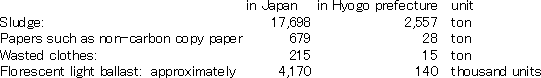
Amount of PCB contaminated solid wastes in Japan and Hyogo prefecture is estimated as below.
Additionally to those four items, low voltage transformers, low voltage capacitors, small electric devices, and storage containers of them are included in the target item. Following is under investigation in Hyogo prefecture and result will be reported in early 2003 fiscal year.
- Each amount of these wastes
- Actual circumstance of storage
- Amount of PCB in these wastes
- Other ingredient in these wastes
2. Extent of proposal
Proposal must be based on developed and corroborated technology that is able to treat these wastes soundly and efficiently. Proposal must satisfy total system of treatment including following,
- Carrying in and storage in the facility
- Pre-treatment
- PCB destruction
- Environment protection measure
- Safety measure
- Recycle or disposal of residue
- Recycle or disposal of treated materials
- Countermeasure of emergency
3. Proposal must satisfy following contents.
(1) Concerning to the proposer
- Representative proposer
- Constituent proposer
- Name of person in charge and contact point
- Holder of the technology which is inducted from others
(2) Concerning to the technology
- Grade of development (Grade of development for practical use)
- Principle of PCB destruction
- Feature and advantage
- Scale up
- Environment protection measure
- Safety measure
- Achievement of treatment
- Patent
- Remarks for reference concerning to the technology
(3) Concerning to the facility
- Explanation of proposal
- Illustration of proposal (arrangement of equipment, flow diagram of main process)
- Cost of construction, cost of operation, etc, according to the treatment capacity of the facility that is assumed 5 to 10tonnes per day.
- Remarks for reference concerning to the facility
(4) Proposal of corroborative experiment
- Is there a facility for a corroborative experiment?
- Request for enforcement of corroborative experiment
- Remarks for reference concerning to the corroborative experiment
(5) Other remarks
4. Method of submission of proposal, time-limit, and address
(1) Method of submission: Proposals must be written in Japanese language only. One printed copy of application forms and relevant documents and additionally, one copy of electronic data of them recorded in a CD-R or CD-RW must be submitted by mail.
(2) Time-limit for submission: application forms, relevant documents and data for the proposal must be arrived before February 26, 2003.
(3) Address: Hyogo Prefectural Environment Create Center Public Corporation
Sakaemachi-Dori, 4-2-18, Chuo-ku, Kobe, HYOGO, 650-0023 Japan
5. Contact point of proposal:
Mitsutoshi Isobe
Deputy general manager of R&D division
Hyogo Prefectural Environment Create Center Public Corporation
Sakaemachi-Dori, 4-2-18, Chuo-ku, Kobe, HYOGO, 650-0023 Japan
TEL: +81-78-360-1308
FAX: +81-78-360-1338
E-Mail: m-isobe@kancri.or.jp